Hello, @bdring, @MitchBradley.
This is stepper’s code using I2S.
I think that it is not fully incorporated into stepper.cpp and still needs to be tested and modified.
I’m happy to share the code with you in order to review and organize the new STEPPER code.
Thank you.
评论 (30)
#2 – odaki 于 2020-04-12
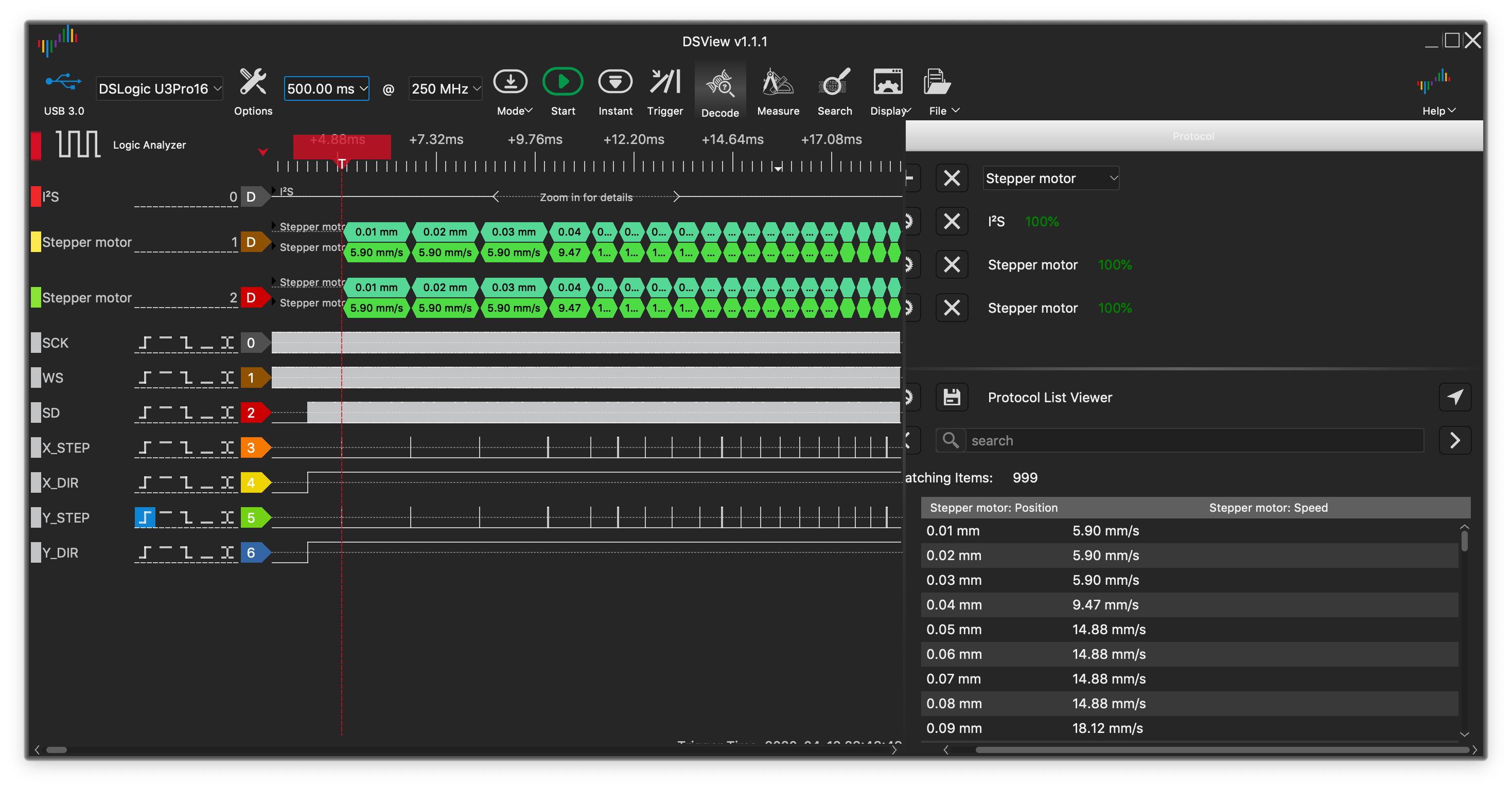
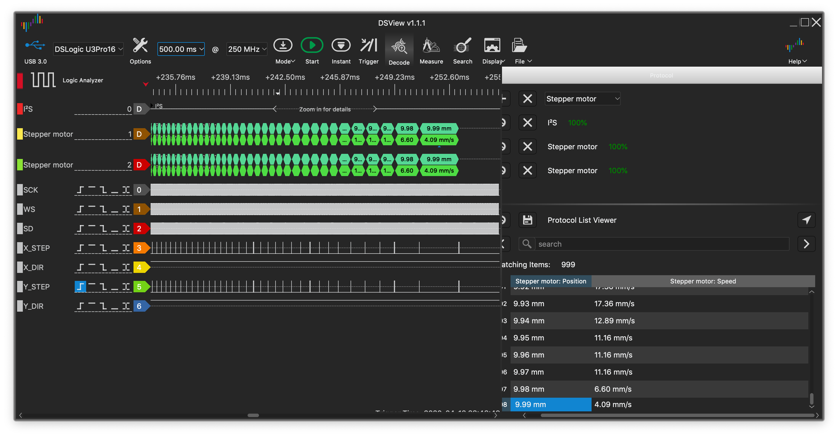
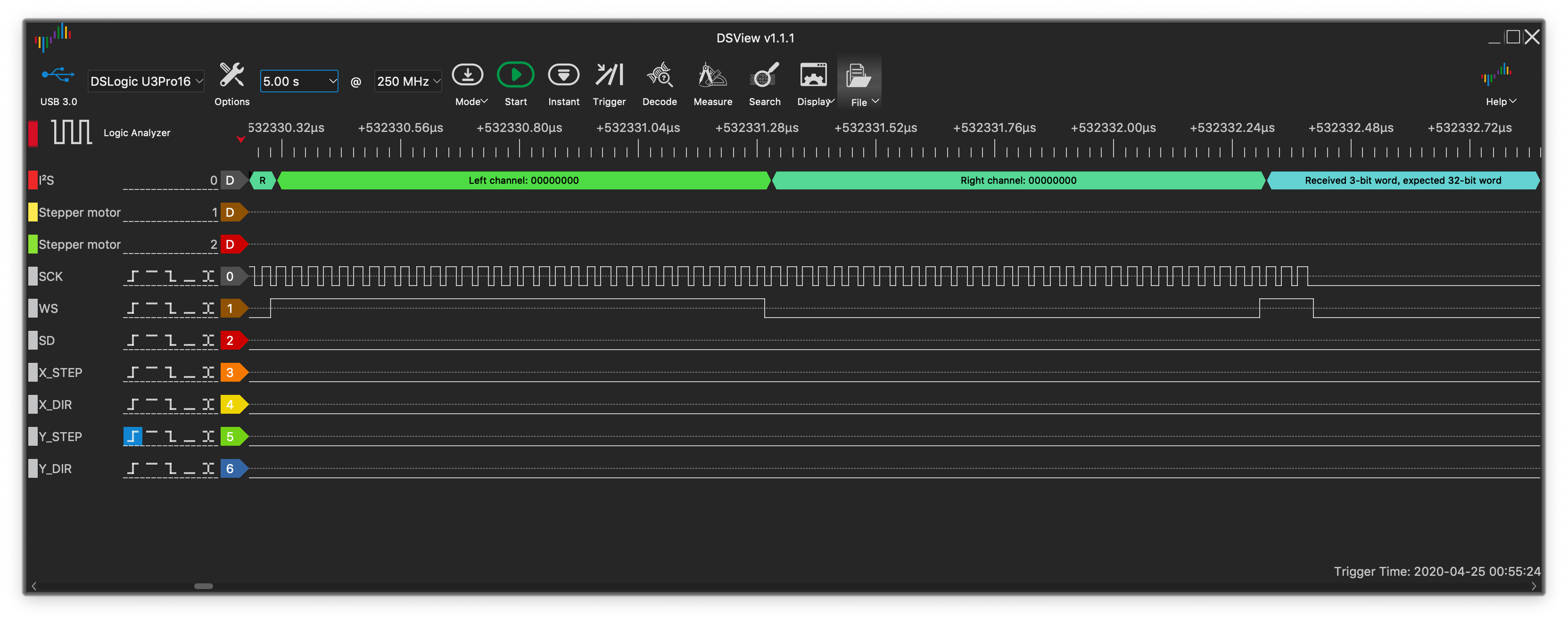
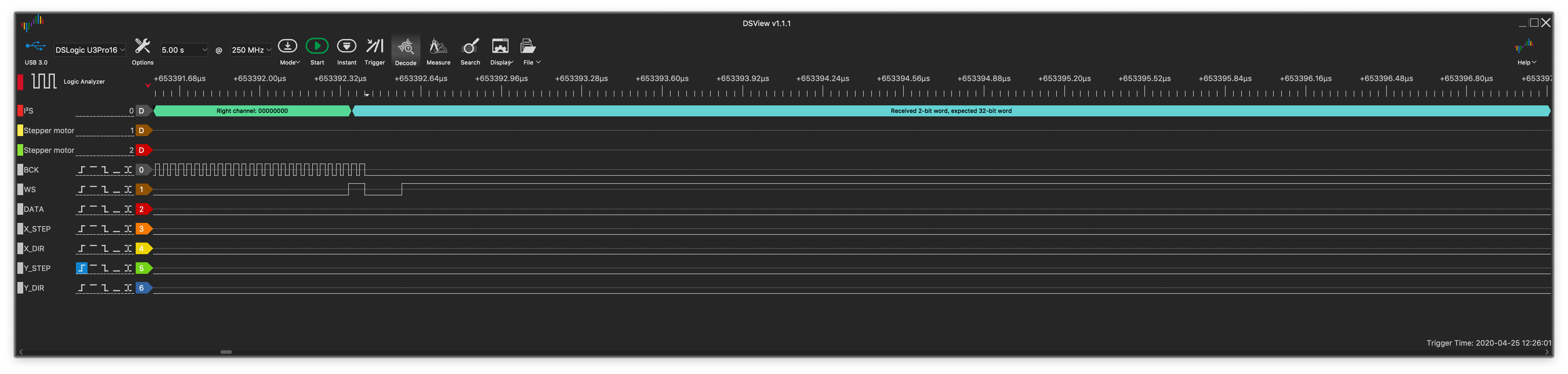
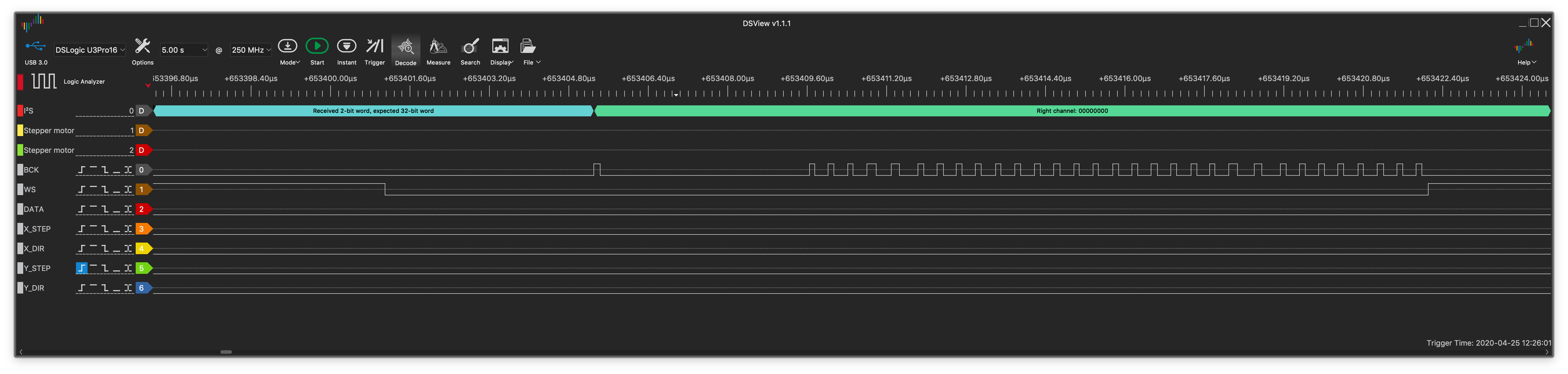
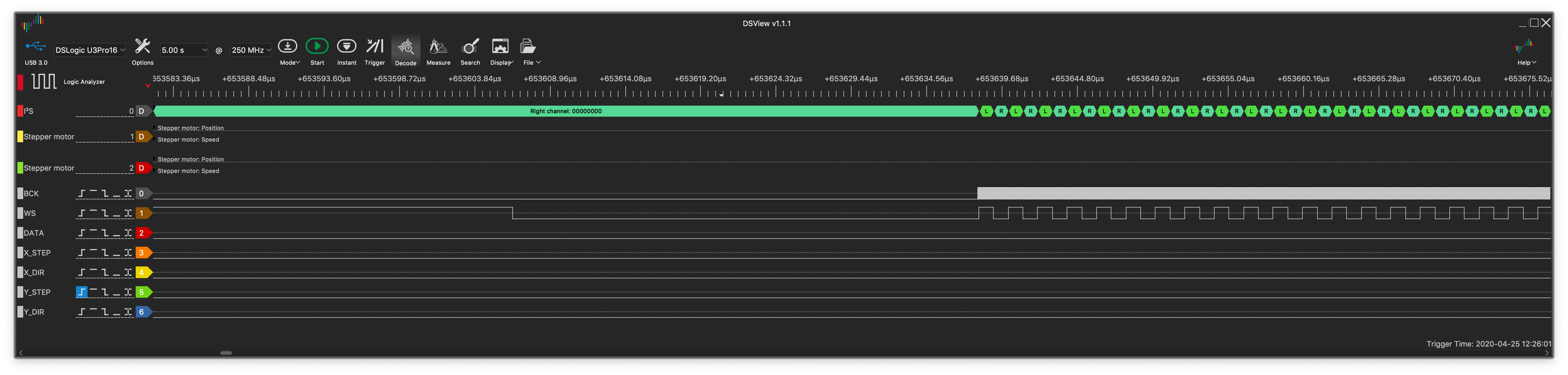
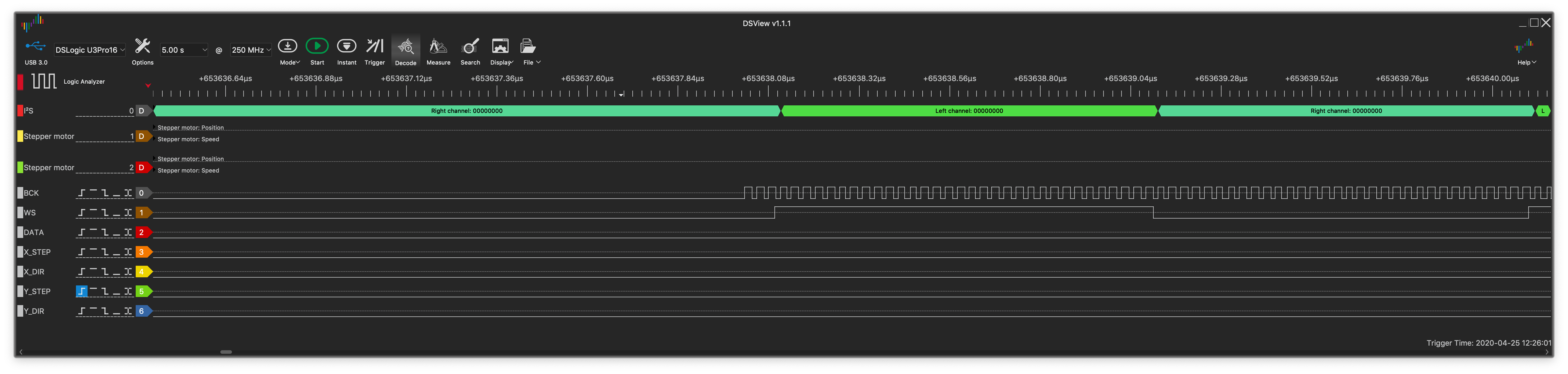
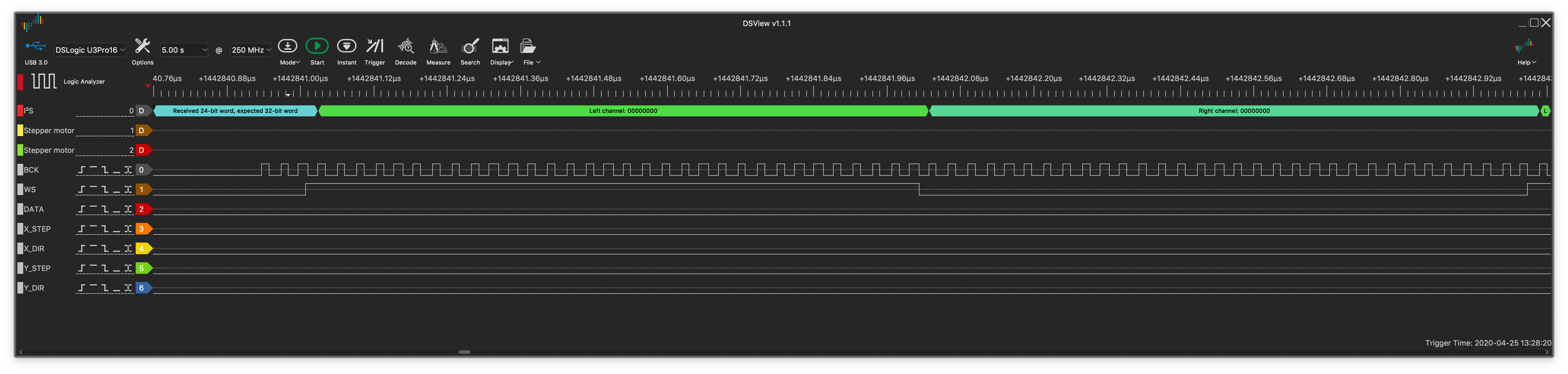
I2S pulse example:
“G0X0Y0” from X10,Y10.
(steps/mm = 100, pulse width = 4us)
#3 – Aggebitter 于 2020-04-23
This is all ready implemented in Marlin 2.0 and started at https://github.com/simon-jouet/ESP32Controller/issues/4′
Take a look in that
#4 – MitchBradley 于 2020-04-23
> This is all ready implemented in Marlin 2.0 and started at simon-jouet/ESP32Controller#4′
> Take a look in that
One guess as to where we started. Hint: https://github.com/MitchBradley/Esp32PrinterController and follow the attribution links.
#5 – odaki 于 2020-04-23
@Aggebitter
Thank you for your comment.
As you can see from the comments and commit history at the beginning, this is a port from Marlin.
Minor modifications such as support for 32-bit expander and a faster bit clock.
#6 – odaki 于 2020-04-23
Now I’m trying to figure out how to stop the transfer cleanly with an emergency stop, etc.
This is because a sudden i2s stop will send half-hearted bits of data to the I/O Expander.
#7 – MitchBradley 于 2020-04-23
I believe that the following procedure will work to establish a specific set of bits at the shift register output:
– Turn off interrupts
– Write 0 to the WS gpio so the next step will immediately drive the WS output low.
– Set the pins back to GPIO mode with
“
gpiomatrixoutcheck(initparam.data_pin, 0x100, 0, 0);

gpiomatrixoutcheck(initparam.bck_pin, 0x100, 0, 0);

gpiomatrixoutcheck(initparam.ws_pin, 0x100, 0, 0);
When this happens, there will be no more rising edges on WS, so updates of the shift register output registers will stop. The data in the output register will be a valid sample from the DMA stream. We do not know which sample, only that it was one of the samples from the stream. The data in the shift registers is indeterminate. It is probably a misaligned sample but that is okay so long as we do not transfer it to the output register.
– From now on we will use programmed I/O – explicit GPIO operations – to perform the following steps:
1. Issue two clock pulses on the BCK pin with the data pin held low. This will deglitch the shift register clocks, in case the switchover to GPIO mode caused a partial clock cycle.
2. Issue 16 (or 24, or 32, depending on the length of the shift register chain) clocks, while shifting in the desired data pattern for the stop condition. Any leftover data from the interrupted I2S operation will thus disappear out the end of the shift register chain.
3. Drive WS high to transfer that shifted-in data to the output register. At this point, the outputs will have the desired state.
– Turn off the DMA, clear the FIFO, etc.
– Turn interrupts back on
– To restart, just reinit the i2s mechanism.
#8 – odaki 于 2020-04-24
Thank you Mitch-san.
If I can tolerate a momentary glitch, I think I can get the I/O Expander back to normal using the method Mitch-san has shown me.
I’m a bit of a paranoid person, so I’m trying to figure out if I can have complete suppression of glitch data.
The role of the DMA is to continuously transfer data to the FIFO, which can hold up to 64 samples.
When the DMA is stopped, the data supply to the FIFO is stopped, but the sample data in the FIFO continues to be output from the Tx module.
If I can stop DMA and allow 64 samples (2us x 64 = 128us in my current implementation) to take extra time, I can stop it without creating a glitch.
In addition, FIFO has a threshold value for transmission (default value is 32, which is half of fullness), so I think it is possible to stop the transmission shorter by controlling this threshold value.
In any case, I need to see how the ESP32 works, so I’m going to test it on the actual machine this weekend.
#9 – MitchBradley 于 2020-04-24
I don’t understand what kind of glitch you are worried about. If you drive WS low then the state of the output pins will be the last sample that was clicked into the output register. Then when you manually clock in the idle value that too will be a valid state. There could be a final step pulse that lasted longer than usual but I have not heard of steppers drivers that are unhappy with long pulses – and the long pulse will not be more than a few microseconds anyway. I cannot think of a situation where an output pin that controls, say, a fan or a heater, would glitch to an invalid state. If the DMA were in the process of turning it on, the shutdown could cause it to be on for less time than otherwise, but that does not seem so bad, and it could happen with a FIFO drain shutdown too. I think that any shutdown method that takes less that a couple of milliseconds will be good enough, so any method you choose will be okay
#10 – odaki 于 2020-04-24
I’ll write a little more about it because I may not be explaining it well enough.
When I observed it last week, when the TX module was sending a few bits of data with WS in LO, and I had to stop I2S, the BCK didn’t stop immediately and the subsequent bits of data seemed to be sent with 0. I said that this unintentional 0 transmission is a glitch.
I think it would be a solution for glitch deterrence if the pin assignment changes that Mitch-san gave me would allow I2S BCK, WS, and DATA to stop at the same time.
I’m trying to verify various actual operations, including this kind of operation, on an actual machine this weekend.
(I am by no means ignoring Mitch-san’s suggestions. I admire you.)
#11 – MitchBradley 于 2020-04-24
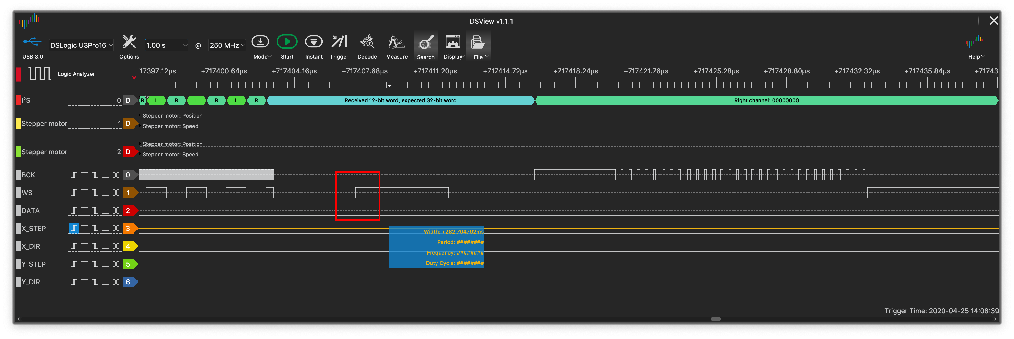
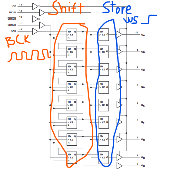
Okay, so I suspect there is an aspect of the 74AHCT595 chips that you might not know about.
!Annotation 2020-04-23 221214
Information is shifted into the Shift register on the left by BCK, but it is only transferred to the Store register on the right – which drives the output pins – when WS goes high. When the DMA/FIFO is running, the rising edge of WS is synchronized so that it goes high at exactly the right time – every 16 (or 24 or 32) BCK cycles – so exactly the right data is transferred to the Store register.
If you force WS to stay low, the information in the Store register will stay at the last value that was transferred from the Shift register at the last rising edge of WS before you forced it low. That will be a valid, properly aligned value that was transferred via DMA.
Now, let us assume that BCK is still running for some time after you force WS low. Some unknown number of bits will be shifted into the Shift register – the “glitch” you mention. But those bits will never appear on the output pins because there is no rising edge on WS. When you finally manage to stop BCK and take control of BCK and DATA via GPIO access, there is unknown data in the Shift register, but that is okay. You can just replace it by shifting in 16 bits of good data – the old data will just fall out the end. It doesn’t matter how much old data is there; in every case you just send 16 bits of new data to fill the Shift register (and push the old data out), then set WS high to make a rising edge. The new data is then transferred all at once into the Store register and appears on the output.
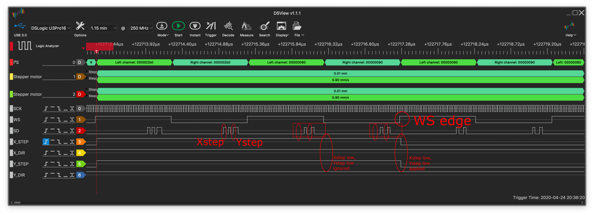
#12 – odaki 于 2020-04-24
I think I’ve identified an important perception difference.
I understand that while WS is LO, the data is taken into 75HC595 at the rising edge of BCK where the value of DATA corresponds to Q0~, and the taken data is reflected in Q0~ at the edge where WS becomes HI.
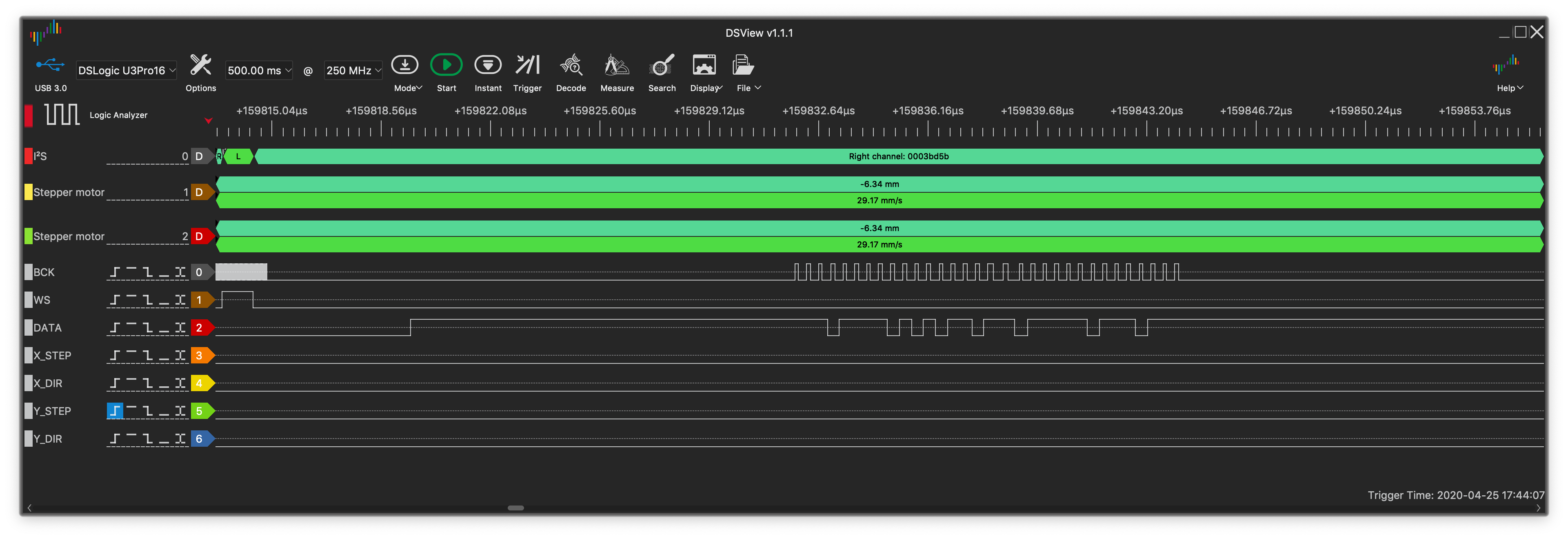
The glitch I saw was that WS was LO and BCK was being output while WS was LO even after a few bits of meaningful DATA had been imported. And after restarting I2S, when WS was first set to HI, it seemed that the unintentional 0 that had been taken in at the time of stopping I2S was reflected in the output of 74HC595.
I have observed with the logic analyzer that if I force WS to be fixed to HI, the DATA is ignored (Therefore, left channel’s data is always ignored)
I’ve written a lot, but I think what Mitch-san is really trying to get across to me is that by forcing WS to operate with the highest priority, even if BCK or DATA is output, it can be ignored, so the glitch output can be deterred.
I think Mitch-san’s explanation is getting through to me.
Please, give me time to actually try it out.
Thank you for your continued support.
#13 – odaki 于 2020-04-24
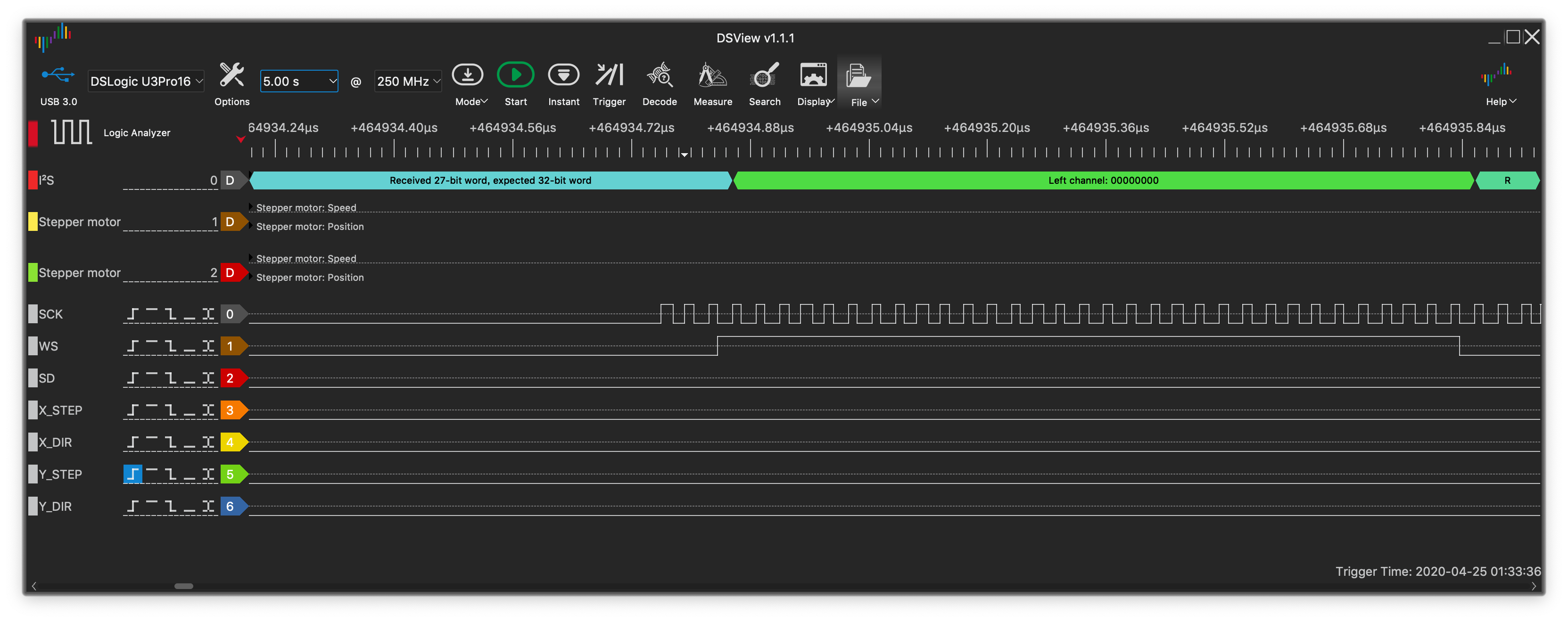
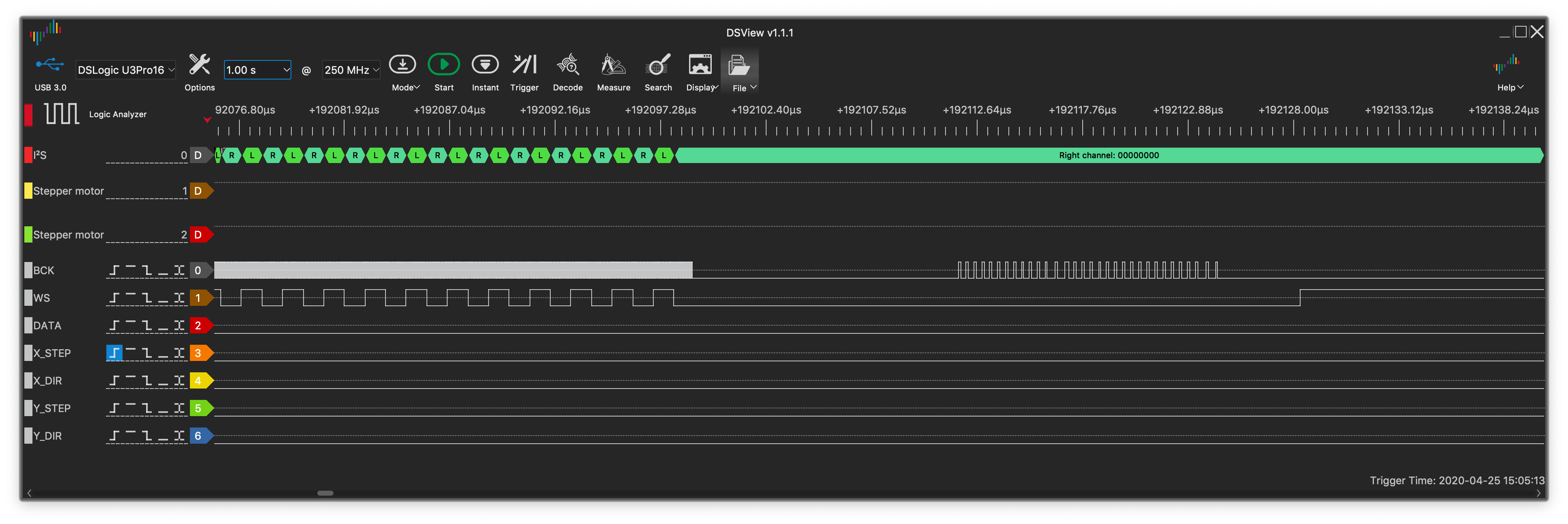
Normal I2S operation.
!text865-4
#14 – odaki 于 2020-04-24
Perhaps I understood what you described in the last paragraph as a recovery method.
The data imported by the 74HC595 is shifted from Q0 to Q1 and from Q1 to Q2 each time it is imported, so even if some data is imported in the middle of the process, it is possible to feed in 32 bits of meaningful data later and then finally latch operation (WS LOW to HI) to make the last 32 bits sent in effective.
This is what I did not understand.
Thank you so much for explaining it to me.
#15 – odaki 于 2020-04-24
I understood that the short answer is this.
If I wanted to stop I2S in an emergency, I would disconnect I2S from the GPIO.
Then, depending on the state of the WS at the emergency stop, the subsequent processing is changed.
If WS is LOW:
– First of all, I have to keep the WS to Low somehow.
– And then empty the FIFO by emptying it or resetting it. (keep the WS to low)
– Control BCK and DATA to send meaningful data for recovery. (keep the WS to low)
– Now, control WS to High and apply meaningful data to 74HC595.
If WS is HIGH:
– First of all, I have to keep the WS to HIGH somehow. —> do not need
– And then empty the FIFO by emptying it or resetting it. (keep the WS to HIGH) —> It was wrong understanding. It needs WS’s edge trigger(LOW to HIGH)
#16 – odaki 于 2020-04-24
@MitchBradley
Thank you for patiently explaining the logic to me.
#17 – odaki 于 2020-04-24
“C++“
static int i2s_stop() {
I2SENTERCRITICAL();
// stop FIFO DMA
I2S0.out_link.stop = 1;
// wait for Idle
while (!(I2S0.state.tx_idle)) {
NOP();
}
// stop TX module
I2S0.conf.tx_start = 0;
//clear pending interrupt
I2S0.intclr.val = I2S0.intst.val;
I2SEXITCRITICAL();
return 0;
}
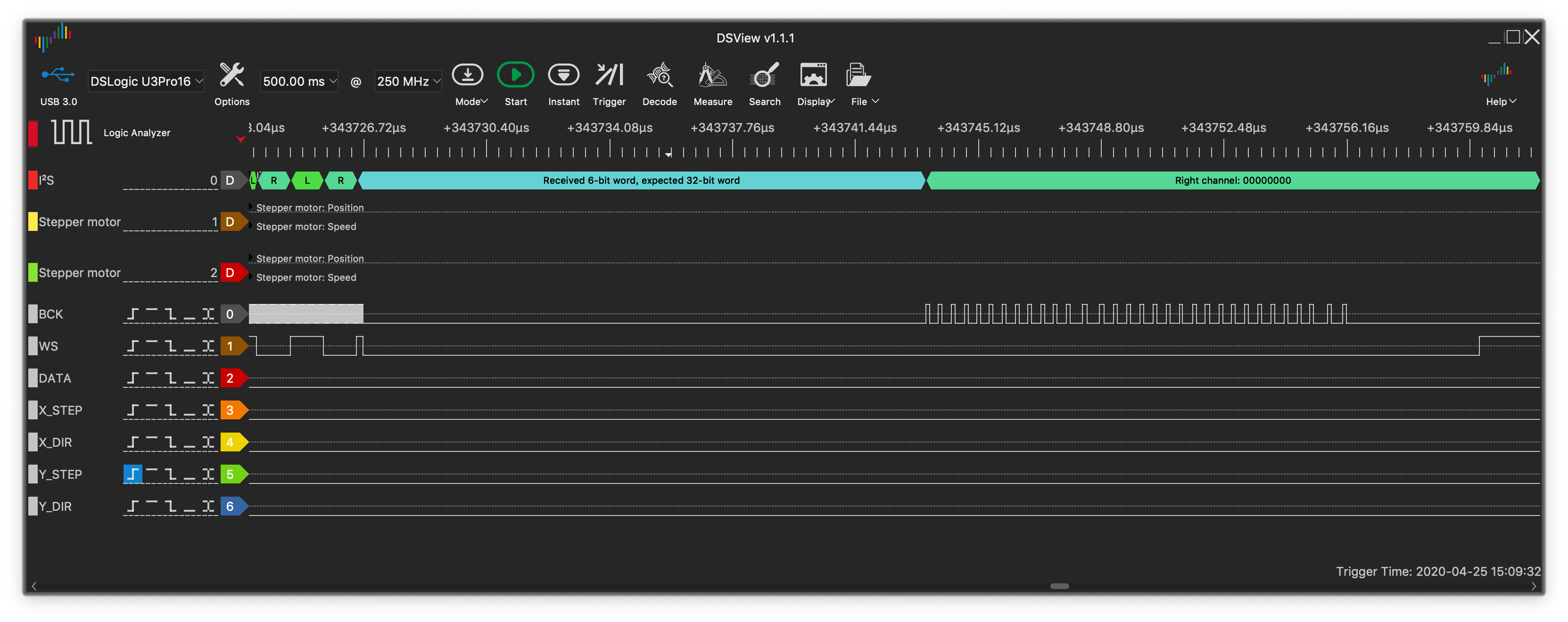
Example 1: If a soft reset occurs when WS is HIGH (it resets without any problem)
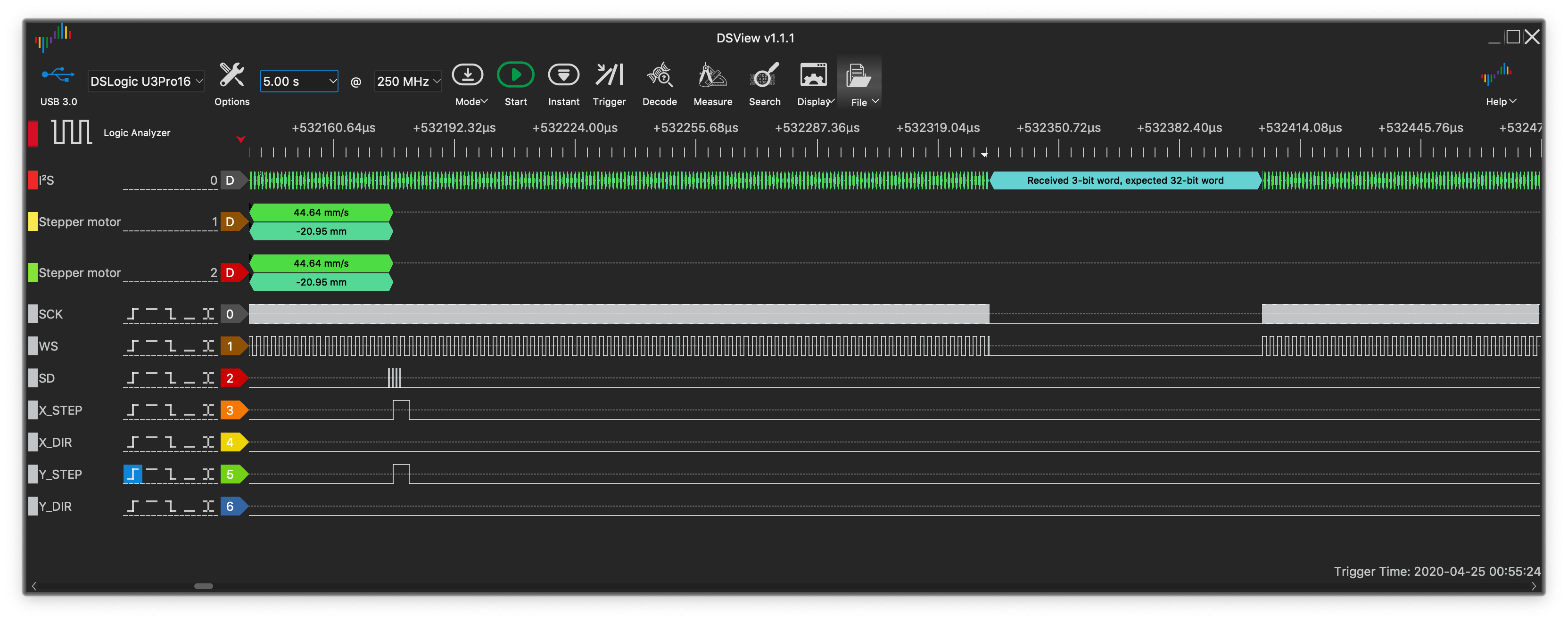
Zoom-up: sent only 3-bits (but ignored because WS is HIGH)
Example 2: If a soft reset occurs when WS is LOW (it sends only 24-bits to the 74HC595)
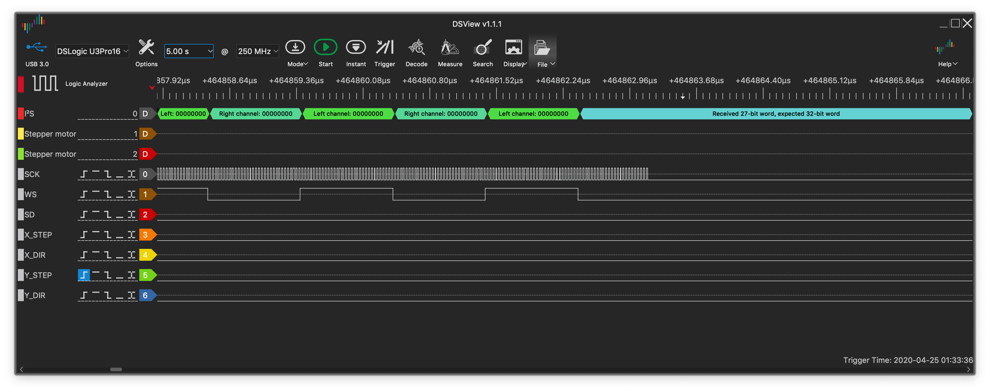
and even though I reset both FIFO and DMA, when I restarted I2S, I got a 3-bits BCK that I don’t understand.(It seems that some kind of initialization is lacking)
#18 – MitchBradley 于 2020-04-24
I think we are coming to a shared understanding! There is one more subtle point about how the ‘595s work: They do not “ignore” BCK while WS is high. The Shift portion responds only to BCK (SRCLK, pin 11), while the Store portion responds only to WS (RCLK, pin 12). The flip-flops in both sections are “edge triggered”, which means that they change state only on the transition from low to high. They are not sensitive to the state, only to the edge.
The “left channel” data, sent while WS is high, is shifted in to the Shift section, but it never appears on the output because it is replaced – shifted out the end – by data from the right channel before WS goes high. When WS does go high, the last N bits (N = length of shift register chain) are still in the Shift section, and are moved to the Store section where they appear on the output.
With the timing shown in the Zoom-up, 64 bits of data are transferred into the Shift chain, but only the last N of them matter. With that timing, it would be possible to have 64 output bits, using a chain of 8 74AHCT595s. 32 of the bits would be sent as left channel data, and 32 as right channel data.
Alternatively, if you were to send 8 bits in the left channel and 8 bits in the right channel at that BCK rate, you could run a two-chip, 16-bit chain at 500 ns per frame, for a 2 MHz step rate! But going that fast would be overkill. The pulses would be too short for many stepper drivers, and the motion planner might have a hard time keeping up.
#19 – odaki 于 2020-04-25
Thank you Mitch-san.
I understood that whether the WS is HIGH or LOW, the data is passed and the last 32 bits are adopted at the edge where the WS is HIGH.
The stop codes I’m currently trying are as follows:
“C++
static int i2s_stop() {
//
// XXX Do not use the raw definitions defined in the machine headers.
//
I2SENTERCRITICAL();
// Stop FIFO DMA
I2S0.out_link.stop = 1;
// Wait for idle
while (!(I2S0.state.tx_idle)) {
NOP();
}
// stop TX module
I2S0.conf.tx_start = 0;
// Detach GPIO pin from I2S
gpiomatrixout(I2SIOEXPANDERWS, 0x100, 0, 0);
gpiomatrixout(I2SIOEXPANDERBCK, 0x100, 0, 0);
gpiomatrixout(I2SIOEXPANDERDATA, 0x100, 0, 0);
uint32t portdata = atomicload(&i2sport_data);
// Force BCK to LOW
digitalWrite(I2SIOEXPANDERBCK, LOW);
// Transmit recovery data to 74HC595
digitalWrite(I2SIOEXPANDERWS, LOW);
for (int i = 0; i < 8 * sizeof(port_data); i++) {
// XXX do not use raw defines for machine
digitalWrite(I2SIOEXPANDERDATA, !!(port_data & (1 << i)));
digitalWrite(I2SIOEXPANDERBCK, HIGH);
digitalWrite(I2SIOEXPANDERBCK, LOW);
}
// Latch
digitalWrite(I2SIOEXPANDERWS, HIGH);
//clear pending interrupt
I2S0.intclr.val = I2S0.intst.val;
I2SEXITCRITICAL();
return 0;
}
`
Example: over all (detach, recovery, re-attach, restart)
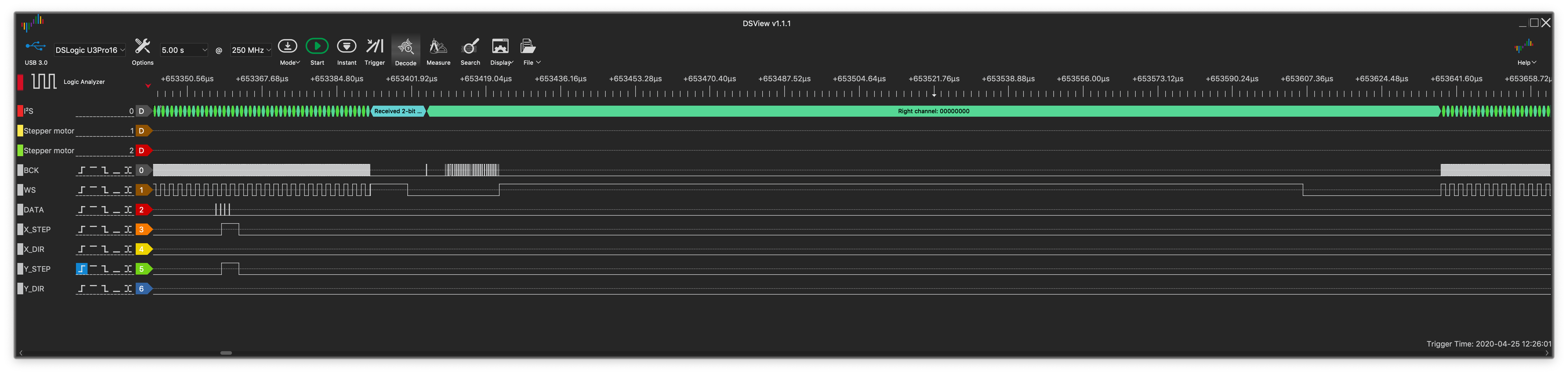
2-bit has sent while WS is HIGH, and I2S detached. For some unknown reason, WS went to HIGH.
I set WS to LOW, and transmit recovery data to 74HC595. Some delay occured between bit0 and bit1 (no problem). Then I set WS to HIGH(edge trigger).
I re-connected the I2S to the GPIO pin again. What appears to be an uneventful recovery, in fact...
When I2S starts working again, I'm getting an unwanted 3-clock BCK and WS edge trigger.
There is probably a problem with the way the I2S restarts, so I'm going to look into this and fix it.
i2s_start code:
`C++
static int i2s_start() {
//
// XXX Do not use the raw definitions defined in the machine headers.
//
i2sgpioattach(I2SIOEXPANDERWS, I2SIOEXPANDERBCK, I2SIOEXPANDERDATA);
//start DMA link
I2SENTERCRITICAL();
i2sresetfifowithoutlock();
//reset DMA
I2S0.lcconf.inrst = 1;
I2S0.lcconf.inrst = 0;
I2S0.lcconf.outrst = 1;
I2S0.lcconf.outrst = 0;
I2S0.conf.tx_reset = 1;
I2S0.conf.tx_reset = 0;
I2S0.conf.rx_reset = 1;
I2S0.conf.rx_reset = 0;
I2S0.int_clr.val = 0xFFFFFFFF;
I2S0.out_link.start = 1;
I2S0.conf.tx_start = 1;
I2SEXITCRITICAL();
return 0;
}
static int i2sgpioattach(uint8t ws, uint8t bck, uint8_t data) {
// Route the i2s pins to the appropriate GPIO
gpiomatrixoutcheck(data, I2S0ODATAOUT23IDX, 0, 0);
gpiomatrixoutcheck(bck, I2S0OBCKOUTIDX, 0, 0);
gpiomatrixoutcheck(ws, I2S0OWSOUTIDX, 0, 0);
return 0;
}
static inline void i2sresetfifowithoutlock() {
I2S0.conf.rxfiforeset = 1;
I2S0.conf.rxfiforeset = 0;
I2S0.conf.txfiforeset = 1;
I2S0.conf.txfiforeset = 0;
}
“
#20 – odaki 于 2020-04-25
I also observe unwanted 3-bit transfers and WS edge trigger when I start running I2S for the first time after a hard reset of ESP32.
There seems to be something wrong with the procedure for starting I2S (even though I’m using the same sequence as the ESP-IDF I2S driver).
Just a thought, there may be a way to prevent unintentional WS edge trigger when starting I2S by using the transfer mode from the right channel.
#21 – odaki 于 2020-04-25
I want to prevent HIGH of WS in the vicinity after I2S detachment,
but I don’t understand why this is happening because I don’t do anything except detachment.
#22 – odaki 于 2020-04-25
By forcibly setting WS to LOW with digitalWrite() just before detaching I2S, I can prevent unintended HIGH of WS.
“C++
static int i2s_stop() {
//
// XXX Do not use the raw definitions defined in the machine headers.
//
I2SENTERCRITICAL();
// Stop FIFO DMA
I2S0.out_link.stop = 1;
// Disconnect DMA from FIFO
I2S0.fifoconf.dscren = 0;
// stop TX module
I2S0.conf.tx_start = 0;
// Force WS to LOW before detach
digitalWrite(I2SIOEXPANDERWS, LOW);
// Detach GPIO pin from I2S
gpiomatrixout(I2SIOEXPANDERWS, 0x100, 0, 0);
gpiomatrixout(I2SIOEXPANDERBCK, 0x100, 0, 0);
gpiomatrixout(I2SIOEXPANDERDATA, 0x100, 0, 0);
uint32t portdata = atomicload(&i2sport_data);
// Force BCK to LOW
digitalWrite(I2SIOEXPANDERBCK, LOW);
// Transmit recovery data to 74HC595
digitalWrite(I2SIOEXPANDERWS, LOW);
for (int i = 0; i < 8 * sizeof(port_data); i++) {
// XXX do not use raw defines for machine
digitalWrite(I2SIOEXPANDERDATA, !!(port_data & (1 << i)));
digitalWrite(I2SIOEXPANDERBCK, HIGH);
digitalWrite(I2SIOEXPANDERBCK, LOW);
}
// Latch
digitalWrite(I2SIOEXPANDERWS, HIGH);
//clear pending interrupt
I2S0.intclr.val = I2S0.intst.val;
I2SEXITCRITICAL();
return 0;
}
“
When detach the I2S at the WS LOW timing.
(Unintended WS edge trigger disappeared.)
When detach the I2S at the WS HIGH timing.
(Unintended WS edge trigger disappeared.)
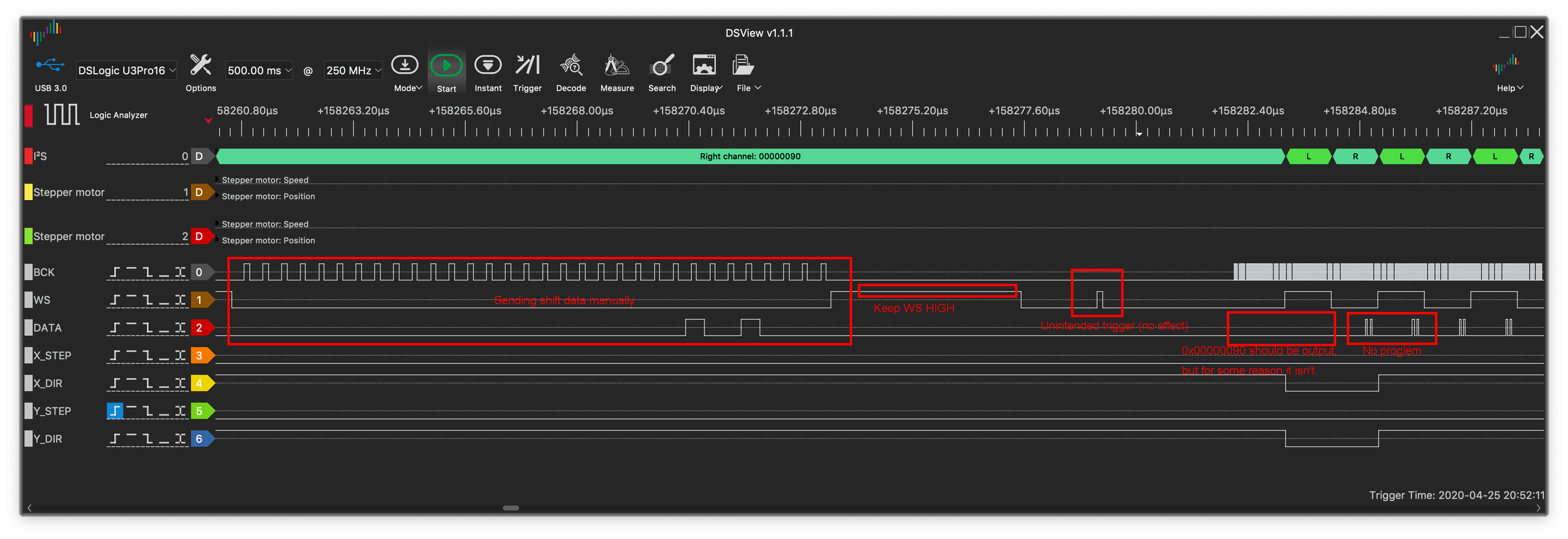
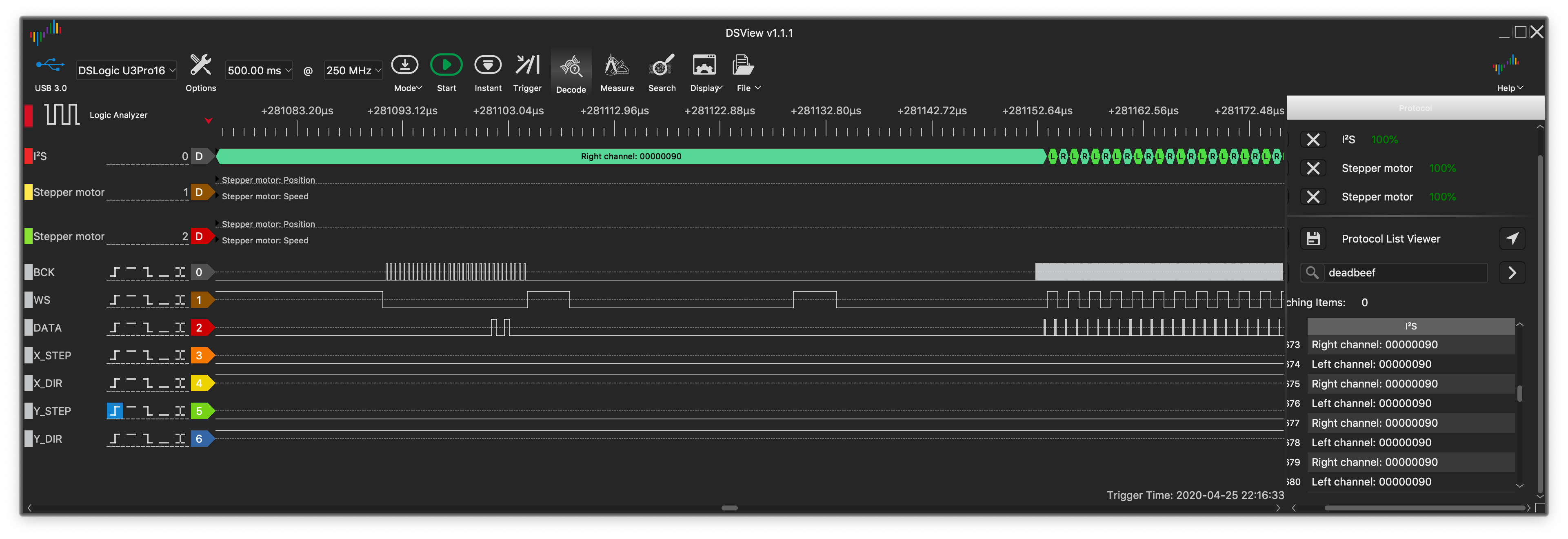
#23 – odaki 于 2020-04-25
I tried to use txstopen to control BCK.
But, It only produced an unintended additional 3-bits, not the intended effect (3-bits of clock suppression).
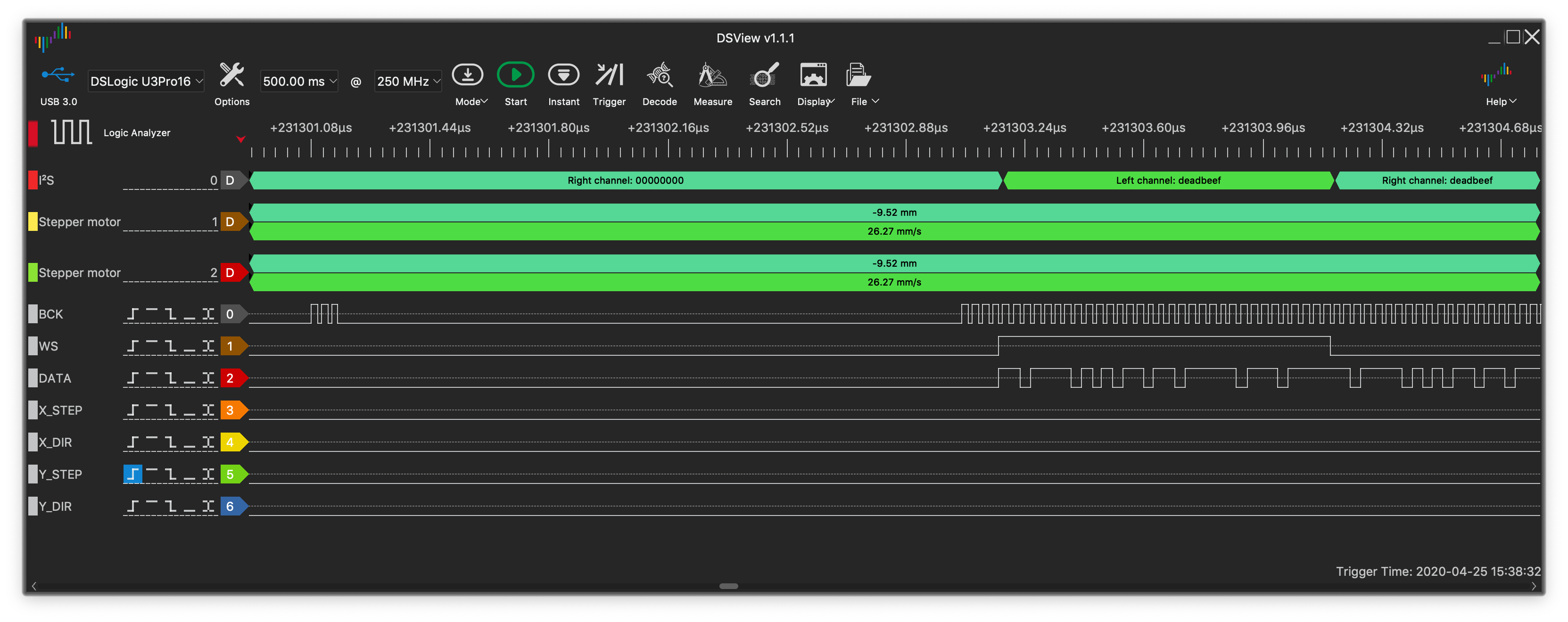
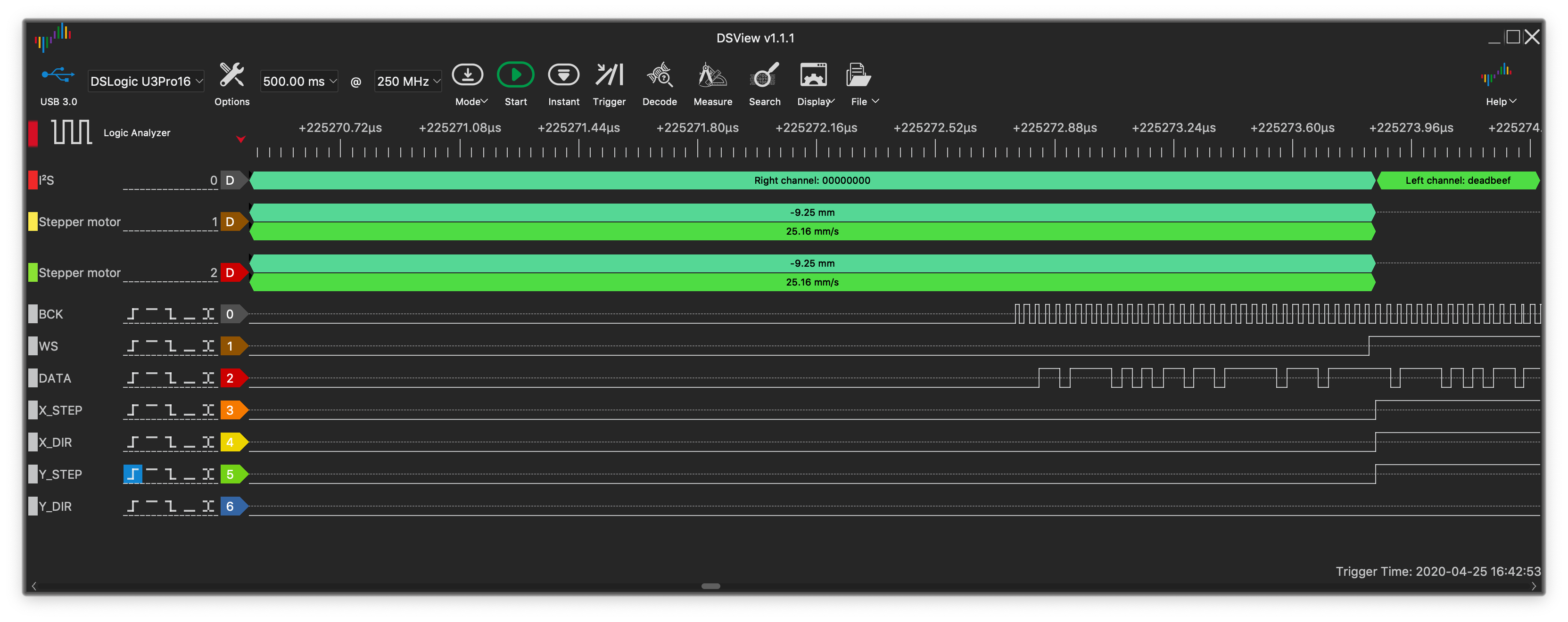
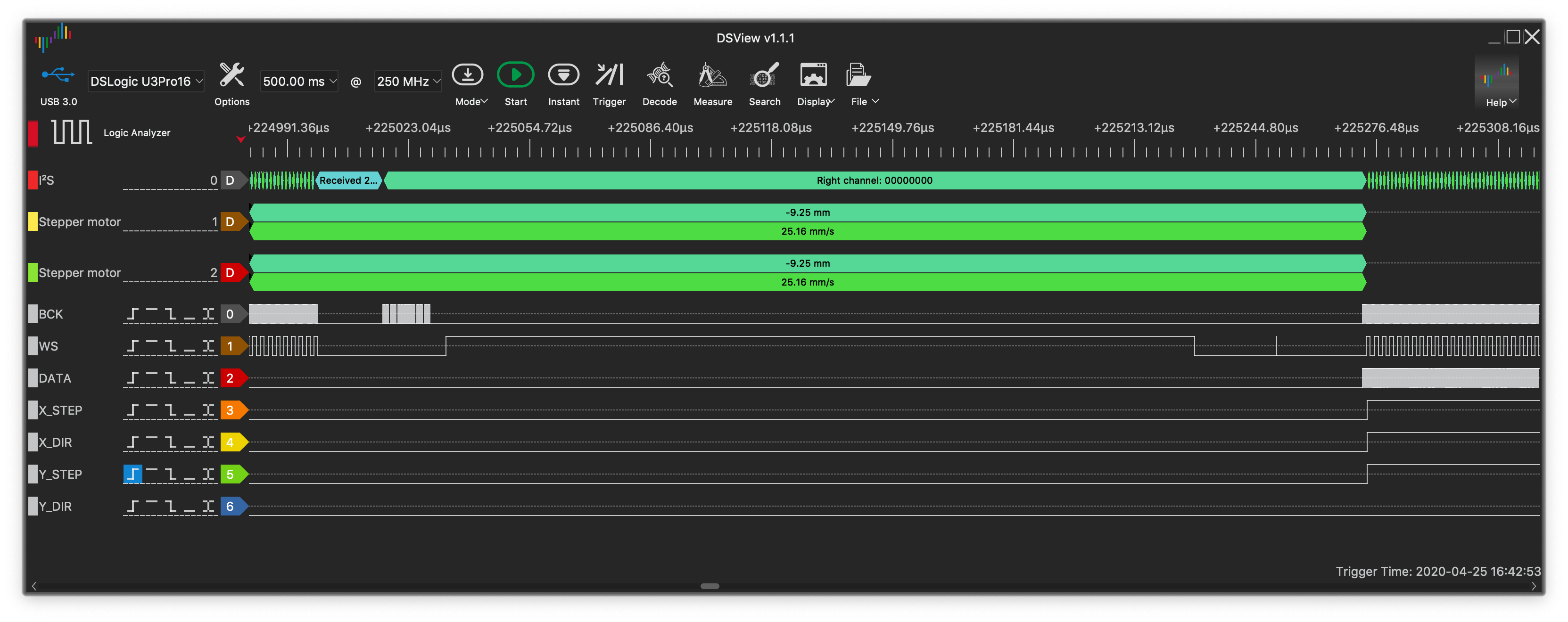
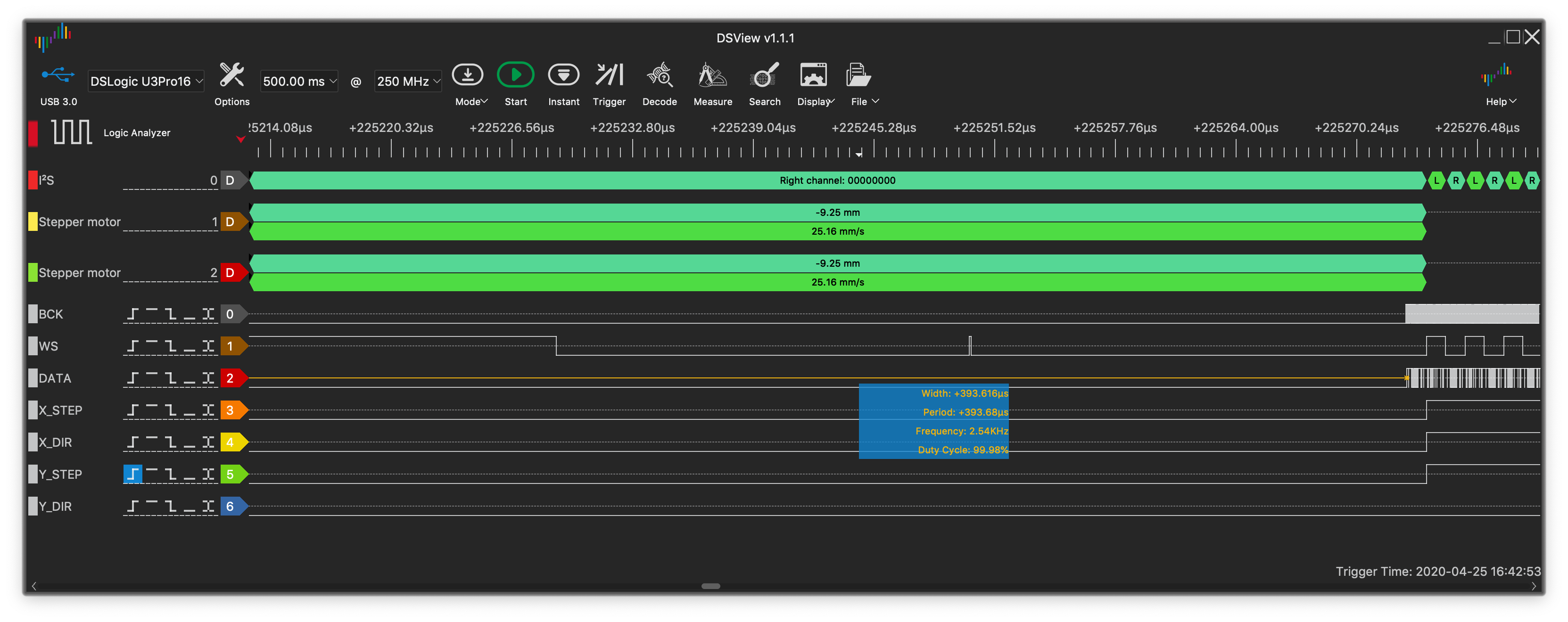
* For testing purposes, 0xdeadbeef is sent as data when I2S resumes.
“C++
static int i2s_start() {
//
// XXX Do not use the raw definitions defined in the machine headers.
//
i2sgpioattach(I2SIOEXPANDERWS, I2SIOEXPANDERBCK, I2SIOEXPANDERDATA);
//start DMA link
I2SENTERCRITICAL();
i2sresetfifowithoutlock();
//reset DMA
I2S0.lcconf.inrst = 1;
I2S0.lcconf.inrst = 0;
I2S0.lcconf.outrst = 1;
I2S0.lcconf.outrst = 0;
I2S0.conf.tx_reset = 1;
I2S0.conf.tx_reset = 0;
I2S0.conf.rx_reset = 1;
I2S0.conf.rx_reset = 0;
// Stop trasmitting BCK and WS
I2S0.conf1.txstopen = 1;
// Connect DMA to FIFO
I2S0.fifoconf.dscren = 1;
I2S0.int_clr.val = 0xFFFFFFFF;
I2S0.out_link.start = 1;
I2S0.conf.tx_start = 1;
// Start trasmitting BCK and WS
I2S0.conf1.txstopen = 0;
I2SEXITCRITICAL();
return 0;
}
“
#24 – odaki 于 2020-04-25
i2s0.conf.txrightfirst has already been set to 1 by i2s_init().
So, change txrightfirst to 0.
This setting seems to do the opposite of the name.
“C++“
I2S0.conf.txmsbright = 1; // Set this bit to place right-channel data at the MSB in the transmit FIFO.
I2S0.conf.txrightfirst = 0; // Set this bit to transmit right-channel data first.
Apparently, this will allow me to recover the I/O Expander state correctly.
#25 – odaki 于 2020-04-25
On closer inspection, there was an unintended WS edge trigger before I2S resumed.
#26 – MitchBradley 于 2020-04-25
You could try preloading the shift registers with the idle data pattern – using programmed I/O on BCK and DATA – prior to initializing the DMA engine. That way, if WS does glitch high before the real BCK starts, the data that will be transferred to the Store registers will be safe. You might want to issue a WS pulse manually anyway, just to make sure the output starts at the desired value. Even if there is another spurious WS edge, it won’t matter because it will just transfer the same data as before to the Store register, since there have been no BCK edges to change the shift register data.
Another thing to try is to clock in the idle data, then issue a rising edge on WS and leave it high prior to switching over to I2S mode. That might cause the first transition to be a falling edge.
#27 – odaki 于 2020-04-25
It seems that this unintended trigger can be addressed by using it as a trigger for a data transfer for recovery.
However, upon closer inspection, it appears that the BCK of the shiftout process for recovery is observed 1 clk earlier than expected.
(Is there some sort of out-of-order going on? –> my bug)
“C++
static int i2s_stop() {
//
// XXX Do not use the raw definitions defined in the machine headers.
//
I2SENTERCRITICAL();
// Stop FIFO DMA
I2S0.out_link.stop = 1;
// Disconnect DMA from FIFO
I2S0.fifoconf.dscren = 0; //Unset this bit to disable I2S DMA mode. (R/W)
// stop TX module
I2S0.conf.tx_start = 0;
// Force WS to LOW before detach
// This operation prevents unintended WS edge trigger
digitalWrite(I2SIOEXPANDERWS, LOW);
// Detach GPIO pin from I2S
gpiomatrixout(I2SIOEXPANDERWS, 0x100, 0, 0);
gpiomatrixout(I2SIOEXPANDERBCK, 0x100, 0, 0);
gpiomatrixout(I2SIOEXPANDERDATA, 0x100, 0, 0);
uint32t portdata = 0xdeadbeef;// XXX test data; atomicload(&i2sport_data);
// Force BCK to LOW
digitalWrite(I2SIOEXPANDERBCK, LOW);
// Transmit recovery data to 74HC595
digitalWrite(I2SIOEXPANDERWS, LOW);
for (int i = 0; i < 32; i++) {
// XXX do not use raw defines for machine
digitalWrite(I2SIOEXPANDERDATA, !!(port_data & (1 << (31 - i))));
digitalWrite(I2SIOEXPANDERBCK, HIGH);
digitalWrite(I2SIOEXPANDERBCK, LOW);
}
// Latch (XXX commented out temporary)
// digitalWrite(I2SIOEXPANDERWS, HIGH);
// digitalWrite(I2SIOEXPANDERWS, LOW);
//clear pending interrupt
I2S0.intclr.val = I2S0.intst.val;
I2SEXITCRITICAL();
return 0;
}
“
#28 – odaki 于 2020-04-25
Thank you Mitch-san.
I’ll give it a try.
#29 – odaki 于 2020-04-25
When restarting I2S, only one sample of unintended 0 data seems to be output.
(Xdir = 1, Ydir = 1 –> 0x00000090 is my expectation)
If I can solve this problem, everything will be just as it should be.
I’m going to commit the source as of today.
#30 – odaki 于 2020-04-25
I got it!
By controlling I2STXSTOPEN in I2SCONF1_REG, I was able to suppress the unintended 0 data at the beginning of I2S stream.
Even after an emergency reset of I2S, Xdir and Ydir continue to be maintained as intended.
If I were to connect my other important devices to I/O Expander, I think I would have been able to prevent them from making unintended movements due to the effects of the reset.
![[gnea/grbl-Mega Issue#1] $ command extentions](https://www.grblhal.com/wp-content/themes/gitphp/timthumb.php?src=https://www.grblhal.com/wp-content/themes/gitphp/assets/img/pic/9.jpg&h=110&w=185&q=90&zc=1&ct=1)
![[gnea/grbl-Mega Issue#2] Better interrupt priorities](https://www.grblhal.com/wp-content/themes/gitphp/timthumb.php?src=https://www.grblhal.com/wp-content/themes/gitphp/assets/img/pic/10.jpg&h=110&w=185&q=90&zc=1&ct=1)
![[gnea/grbl-Mega Issue#4] Real-time adjustable feedrates](https://www.grblhal.com/wp-content/themes/gitphp/timthumb.php?src=https://www.grblhal.com/wp-content/themes/gitphp/assets/img/pic/6.jpg&h=110&w=185&q=90&zc=1&ct=1)
#1 – odaki 于 2020-04-11
@MitchBradley
As you’ll notice, the cleanup is not enough, so I’m going to do some more code cleaning.